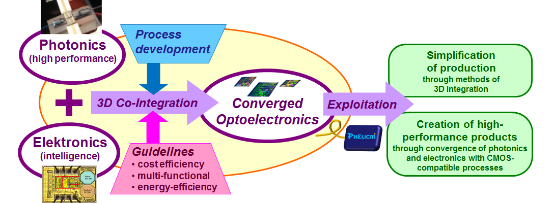
Objective 1. Converged optoelectronic integration on a high functionality silicon platform
PHELICITI will pursue the development of a silicon library for advanced optoelectronic components with transmission, detection and signal manipulation capabilities. A new generation of functional and miniaturized photonic and electronic components and CMOS-compatible waveguide technologies will be developed in order to fabricate miniaturized integrated subsystems-on-chip with small form factor. The overall toolbox used for this purpose will include monolithic integration of passive optical waveguide functionalities, SiGe photo detectors and linear BiCMOS electronic transimpedance amplifiers, silicon ring modulators and SiGe BiCMOS multi-level drivers, and silicon interposer technology for multi-layer 3D integration.
Objective 2. To investigate a set of elements for a library of advanced optoelectronic components with increased flexibility and energy efficiency
PHELICITI will exploit the functional convergence of intelligent electronics with high-speed photonics to offer flexible optoelectronic systems. This incorporates dynamic reconfigurability of the underlying photonic hardware, supervision of optics and re-calibration of subsystems, and smart power management. Optimization in all aforementioned points takes place at the physical chip level rather than on the application layer.
Objective 3. To advance the scale of integration in complex silicon optoelectronic circuits
The developed integration toolbox will be the basic instrument to enable the composition of larger-scale systems such as arrayed transceivers for 8x10 Gb/s. The common integration of transmitter and receiver subsystem on the same chip will be enabled through sophistication of the electro-optic design, battling the inter- and intra-transceiver crosstalk.
Objective 4. To fabricate and experimentally evaluate 3D integrated test-chips
An important aim of PHELICITI is the demonstration of 3D optoelectronic chip integration through a series of test-chips. These chips will be evaluated in laboratory test-beds according to selected applications fields in the telecom and datacom segment. The full library of functional components will be subject to evaluation.
Objective 5. Economic viability of 3D integration methodology
PHELICITI aims at economic viability when applying technology for optoelectronic 3D integration while it targets challenging applications that raise demanding specs for the systems under development.